In the world of electronics, two-dimensional (2D) semiconducting materials have been gaining attention for their unique optoelectronic properties. These materials have the potential to revolutionize the development of ultra-thin and tunable electronic components. However, one of the major challenges researchers have faced is effectively interfacing these materials with gate dielectrics. This has often led to the formation of interfacial traps that degrade the performance of transistors.
A New Approach
A recent study conducted by researchers from King Abdullah University of Science and Technology (KAUST), Soochow University, and other institutions globally proposed a novel approach to tackle this issue. The researchers introduced a design that involves using hexagonal boron nitride (h-BN) dielectrics and metal gate electrodes with a high cohesive energy. By analyzing the interaction between platinum (Pt) anodes and h-BN stacks, they discovered that Pt/h-BN gate stacks showed significantly lower leakage current compared to Au/h-BN gate stacks. This finding spurred the idea of utilizing chemical vapor deposited h-BN as a gate dielectric in 2D transistors.
Experimental Process
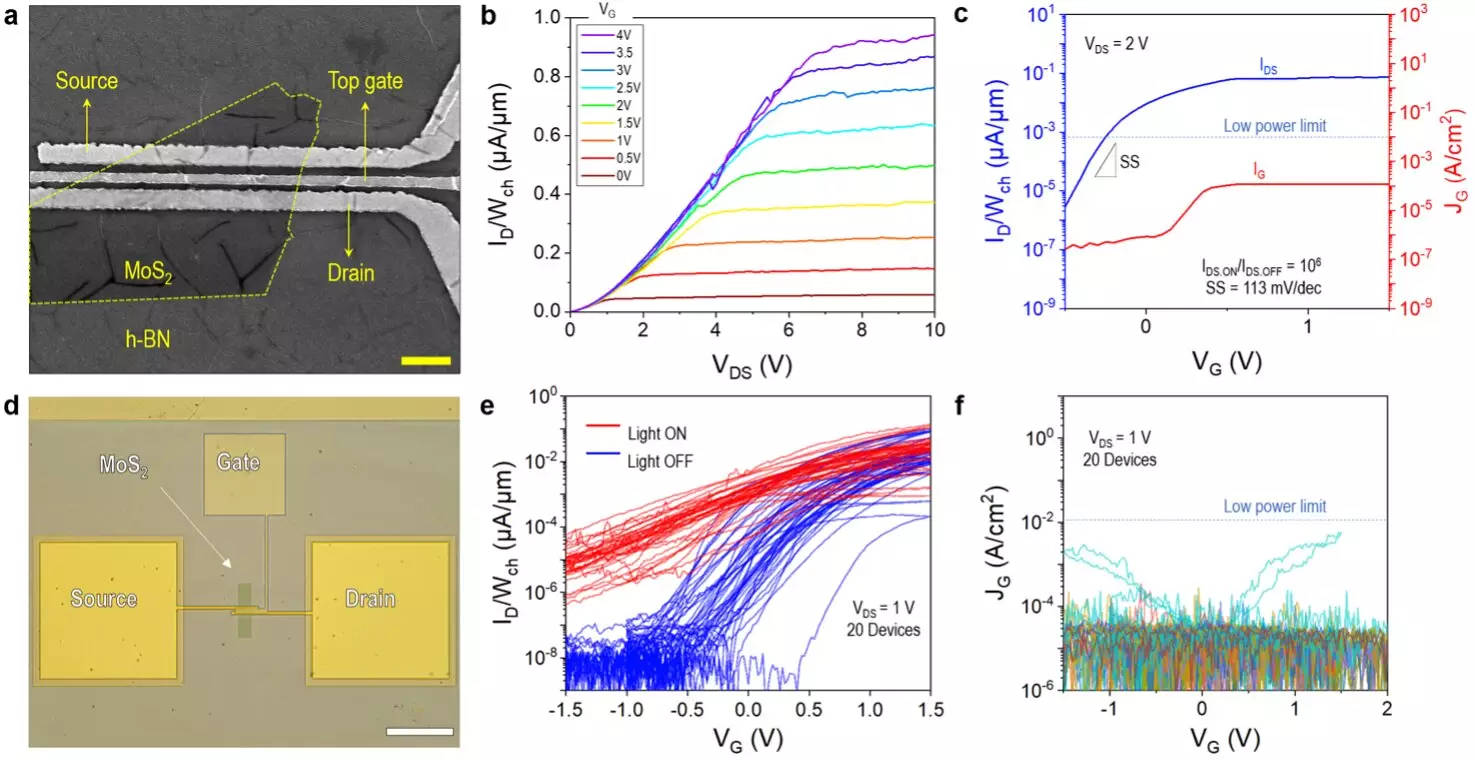
The team led by Yaqing Shen and Prof. Mario Lanza proceeded to fabricate over 1,000 devices using h-BN gate dielectrics and high cohesive energy metals such as Pt and tungsten (W). The fabrication process involved cleaning a SiO2/Si substrate, patterning source and drain electrodes (Ti/Au), transferring MoS2 as the channel material, and depositing CVD h-BN film. The researchers also patterned the Pt gate electrode using electron beam lithography and deposited it using e-beam evaporation. This meticulous process ensured a clean van der Waals interface between MoS2 and h-BN, enhancing the transistor’s reliability and performance.
Contrary to the belief that CVD h-BN is an ineffective gate dielectric, the research team demonstrated that selecting the right metal electrodes, such as Pt and W, enables its successful use in field-effect transistors with MoS2 channels. The clean van der Waals interface between MoS2 and h-BN not only improves reliability but also enhances gate control. The team’s findings suggest that high cohesive energy metals play a crucial role in making CVD h-BN an effective gate dielectric in 2D transistors.
The innovative approach taken by Shen and her colleagues has shown promising results in reducing current leakage and achieving a high dielectric strength of at least 25 MV cm-1. Tests revealed that Pt and W-based gate electrodes significantly decreased the leakage current across h-BN dielectrics compared to traditional Au electrodes. This breakthrough could pave the way for reliable solid-state microelectronic circuits and devices based on 2D materials.
As researchers continue to explore the potential of 2D semiconductor-based transistors, the development of highly performing devices using similar approaches and materials is on the horizon. The work conducted by Shen’s team opens up possibilities for fabricating advanced solid-state electronics with enhanced reliability and performance. Moving forward, the researchers plan to focus on developing ultra-small, fully 2D transistors to further push the boundaries of electronic miniaturization and extend Moore’s Law.


Leave a Reply