The field of electronics engineering has long been searching for materials that can push the boundaries of transistor performance beyond the constraints of silicon-based technology. One of the most promising candidates in this quest is two-dimensional (2D) semiconductors. These materials possess unique properties that could revolutionize the development of high-performance transistors. Notably, 2D semiconductors are atomically thin and exhibit high carrier mobilities, characteristics that have the potential to enhance the electrostatic control and ON-state performances of short-channel field-effect transistors (FETs).
However, despite their advantages, 2D semiconductors face a significant challenge in the form of high contact resistances resulting from Fermi-level-pinning effects. These effects have been a major roadblock in the practical implementation of 2D materials in electronic devices. Recently, researchers at Peking University and the Chinese Academy of Sciences have proposed a novel yttrium-doping strategy to mitigate this limitation and improve the integration of 2D semiconductors in electronics.
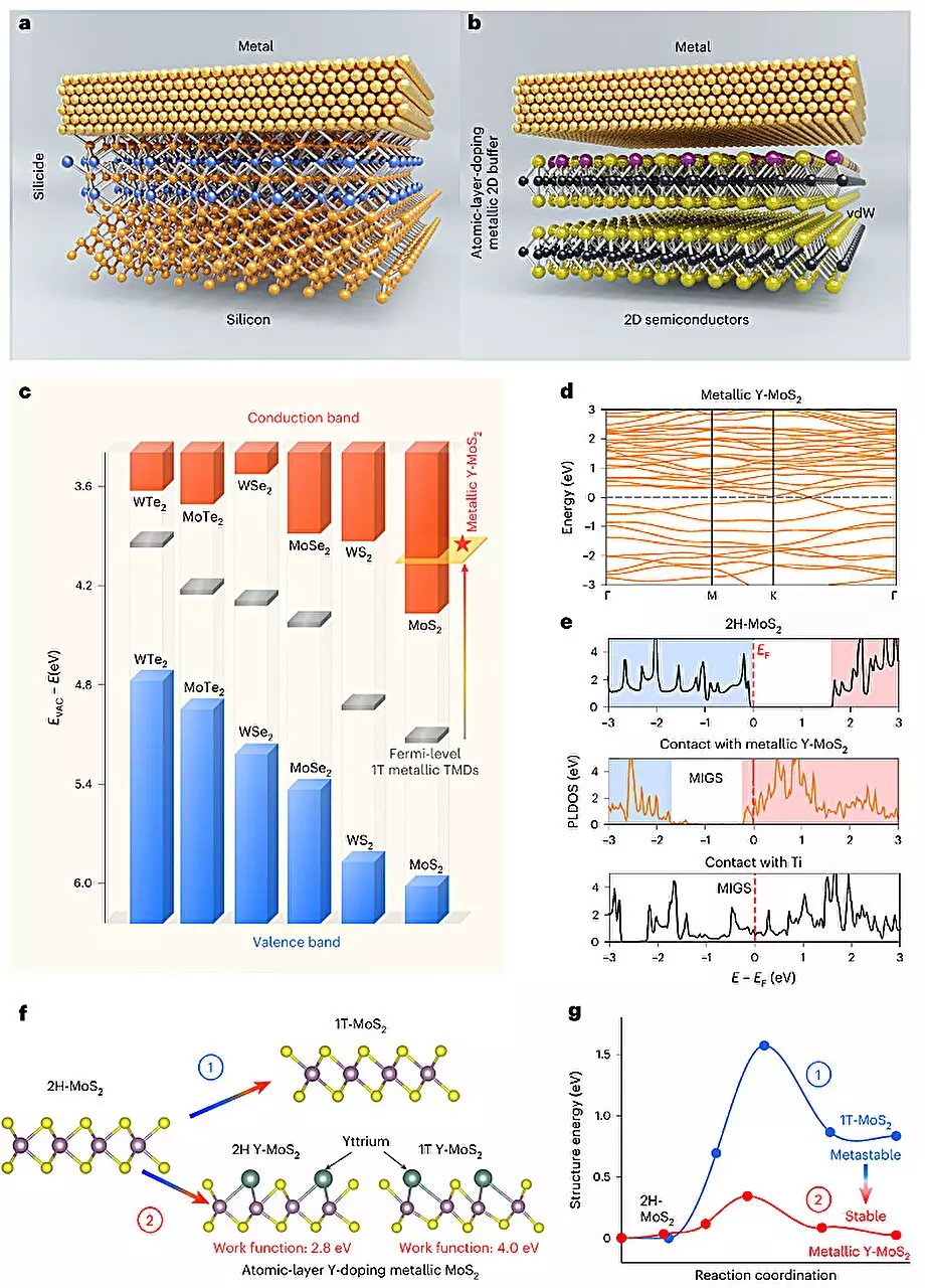
The innovative approach introduced by the research team involves the conversion of semiconducting molybdenum disulfide (MoS2) into metallic MoS2 by incorporating yttrium as a dopant. By placing a semi-metal layer between a metal electrode and the 2D semiconductor, the efficiency of carrier injection from the electrode to the semiconductor is enhanced. This concept draws inspiration from the traditional silicide structures employed in silicon-based transistors.
A key objective of the study was to tackle the Fermi-level pinning effects that hamper the performance of 2D transistors. The plasma-deposition-annealing (PDA) method was utilized to achieve yttrium doping in MoS2. By generating active sites through low-power plasma treatment and depositing a Y/Ti/Au stacked metal, the researchers were able to successfully dope MoS2 with yttrium atoms, ultimately improving band alignment and facilitating the fabrication of ohmic contacts for 2D transistors.
The researchers introduced a groundbreaking concept termed “rare earth element yttrium doping-induced 2D phase transition,” which describes the metallization effect observed in MoS2 upon yttrium doping. This approach represents a significant leap in the field of semiconductor doping, allowing for selective-area single-atomic-layer surface doping with unprecedented precision. The doping depth achieved through this technique is an impressive 0.5 nanometers, surpassing traditional limitations in ion implantation doping.
As a result of their yttrium-doping strategy, the research team successfully developed ultra-short MoS2-based channel ballistic transistors with excellent ohmic contacts and superior switching capabilities. These advancements pave the way for the production of sub-1 nanometer node chips with exceptional performance metrics and reduced power consumption. Moving forward, the researchers aim to further refine their approach to develop equally effective p-type ohmic contacts for 2D semiconductors, pushing the boundaries of transistor technology even further.


Leave a Reply